
Built for Precision, Engineered for Excellence
Vertel Digital’s manufacturing facility represents the pinnacle of Indian engineering excellence. Located in the industrial hub of Gujarat, our 50,000 sq.ft facility is equipped with cutting-edge equipment and processes that enable us to produce world-class wireless communication products that compete with global brands.
Category 1 DMR
Manufacturer
Globally recognised by the DMR Association
Full Product
Range In-house
Handheld, Mobile, Base & Repeater radios, all manufactured under one roof
MIL-STD 810 &
IP68 Compliant
Devices engineered and tested to military-grade durability and ingress protection standards
BIS Approved Products
Every product meets Bureau of Indian Standards requirements and is ready for India’s most demanding sectors.
Production Zones
Dedicated areas optimised for every stage of the digital radio assembly process.
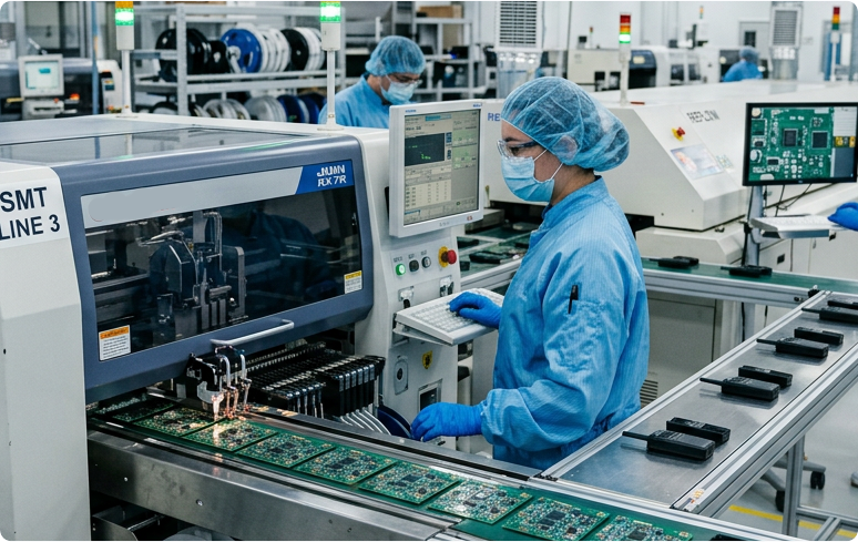
RADIO ASSEMBLY ZONE
Precise, structured assembly for mission-critical radio performance
Our radio assembly zone is the heart of the Vertel manufacturing process. Staffed by trained technicians with deep expertise in radio hardware, this zone handles the careful integration of all mechanical, electronic, and RF components into finished handheld, mobile, base station and repeater units. Every assembly follows strict build specifications to ensure consistent performance across all product lines.
- Structured assembly of handheld, mobile, base station, and repeater radios
- VHF and UHF frequency-band specific hardware integration
- Housing, antenna, battery, and peripheral assembly
- Inline quality checks at every assembly stage
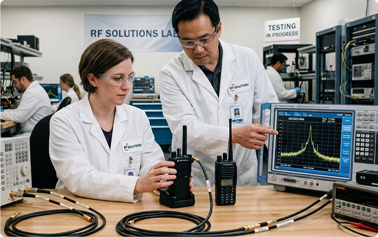
TESTING LABORATORY
Comprehensive RF and functional testing with advanced equipment.
Every Vertel radio undergoes rigorous RF and functional testing before it leaves the facility. Our testing laboratory is equipped with professional-grade RF analysers and protocol testing tools to verify that each product meets DMR standards and performs reliably in the harshest field conditions.
- RF spectrum and signal analysis across VHF & UHF bands
- DMR protocol compliance testing
- Audio sensitivity and clarity benchmarking
- IP rating and ingress protection validation
- Battery discharge and charge cycle testing
Manufacturing Capabilities
Complete in-house manufacturing for all Vertel communication products
Category 1 DMR Manufacturing
Analog Radio Production
PoC Device Assembly
Custom Frequency Programming
Repeater System Integration
Accessory Manufacturing
Battery Pack Assembly
Antenna Production
ESD-Protected Assembly
Custom Branding & Labeling
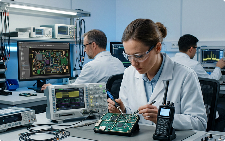
R&D Center
Innovation hub for next-generation wireless communication.
Vertel’s in-house R&D team brings together hardware engineers and firmware developers who push the boundaries of what Indian made radios can achieve. Our R&D capability enables rapid design-to-production transitions and supports our mission of applying European technology standards to products built for Indian conditions.
- Radio hardware design and validation using industry-standard EDA tools
- Firmware development for DMR digital protocols
- RF simulation and frequency optimisation
- New product prototyping and pre-compliance testing
- Open-standard data application development for radio peripherals
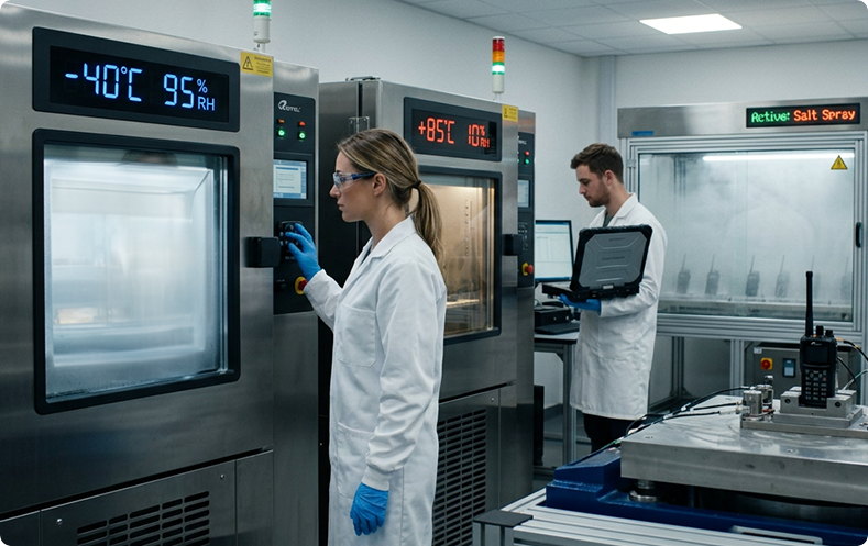
Environmental Testing
Temperature and humidity chambers for reliability testing
Our environmental testing facility ensures every product can withstand harsh operating conditions. We perform accelerated life testing, thermal cycling, and humidity exposure to validate product durability before market release.
- Temperature range: -40°C to +85°C
- Humidity testing: 10% to 95% RH
- Vibration and shock testing
- IP rating validation
- Salt spray corrosion testing
Manufacturing Process
End-to-end assembly with quality checks at every stage
Component Intake & Inspection
Incoming parts and sub-assemblies are verified against the specification before entering the production line
Mechanical Assembly
Housing, chassis and structural components are fitted and secured
Electronic Integration
Radio modules, antennas, batteries and peripherals are installed and connected
Firmware programming
Each unit is programmed with the latest certified firmware and channel configurations
RF & Protocol Testing
100% functional, DMR protocol and RF performance testing across VHF & UHF Bands
Packaging
Quality check, brand labelling, and dispatch-ready packaging
Certifications
DMR Association

BIS

ISO Certification
MIL-STD 810G
ETSI